Introduction
I have been working with the Xilinx ZCU106 Zynq MPSoC development board and I wanted to share my experience designing with the board. The Xilinx ZCU106 evaluation board offers many features including DDR4 memory interfaces, Quad-SPI, SD card and JTAG configuration options, high-speed serial transceivers, video codec unit (VDU), and peripheral interfaces including I2C, SPI, DisplayPort, USB3 etc. It is a great prototyping platform and I am excited to try out different projects using the board.
The project I cover in this post includes using a Digilent Pmod Gyroscope to record angular velocity of an object rotating around its X, Y and Z axes. In this project, the Xilinx ZCU106 development board is designed to continuously read angular velocity data from a Digilent PmodGYRO module using the I2C interface, and display the readings using a GUI application in a host PC.
Parts
Following is the parts list for the project.
- Xilinx ZCU106 Evaluation Board
- Digilent PmodGYRO
- Two (2) USB Type-A to Micro-B cables
- One (1) PC to communicate with the ZCU106 board
A brief description of the board and parts included in the project are below:
I Xilinx ZCU106 Zynq UltraScale+ MPSoC development board
The Xilinx ZCU106 Zynq UltraScale+ MPSoC development board is an evaluation board featuring the xczu7ev-2ffcv1156 device, which combines programmable logic (PL) and a processing system (PS) including a 64-bit quad-core Arm Cortex-A53 based application processing unit (APU), a 32-bit dual-core Cortex-R5F based real-time processing unit (RPU) and a Mali-400 graphics processing unit (GPU), in a single device. Xilinx provides exhaustive documentation for this board. Some of the documents providing invaluable information about all the features on the board are listed under References [1] to [5] and [11] to [13].
II Digilent PmodGyro
The Digilent PmodGYRO is a 3-axis gyroscope module that includes an STMicroelectronics L3G4200D angular rate sensor. This module provides the rate of change of rotation on all 3 axes (X, Y and Z) in 16-bit signed integer (two’s complement) format, that can be communicated to the host board through a user-selectable I2C or SPI interface. The PmodGYRO has 2 headers – a 12-pin J1 header for SPI communication and an 8-pin J2 header for I2C communication.
I used the J2 header and implemented the I2C protocol in the PL side of the ZCU106 board. There is a lot of documentation and sample projects on I2C protocol available online. The documents that I found most useful to get the Pmod working can be found under References [6] to [10].
III Cables and Connectors
The project uses one (1) power cord for the ZCU106 board and two (2) USB Type-A to Micro-B cables, all of which come with the development board.
Setup
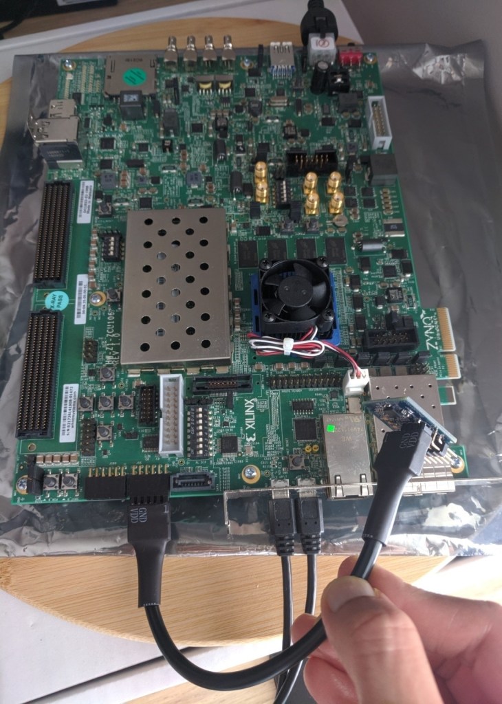
The hardware setup for the project is shown in the figure below.

- First, the Xilinx ZU106 dev board is connected to power supply using a power cord that connects the 6-pin power supply plug to J52. The board can be turned on and off by sliding the SW1 slide switch (Fig 1).
- The USB-UART connector J83 on the ZCU106 board is connected to the PC using a USB Type-A to Micro-B cable (Fig 1).
- The USB-JTAG connector J2 on the ZCU106 board is connected to the PC using a USB Type-A to Micro-B cable (Fig 1).
- The PmodGYRO is connected to the PMOD GPIO header J55 on the ZCU106 board (Fig 1). An extension cable from the Pmod cable kit provided by Digilent could also be used to connect the Pmod to the dev board (Fig 2).

Design
The pmod_iic module is the main module that controls the complete sequence of events. After the ZCU106 board is powered on, and the program is loaded in the processor memory, pushbutton SW18 is pressed once to start data acquisition from the Pmod. The Pmod control registers are set and the status register is polled to check for new X, Y or Z data. When new data is available, the X_L, X_H, Y_L, Y_H, Z_L and Z_H registers are read and stored in the PL BRAM. After 32 writes to the BRAM, the PL issues an interrupt to the PS, and the APU reads data from the PL through the AXI BRAM controller. Data read from the BRAM is transmitted to the host PC via serial UART. A Processing sketch running in the host PC reads UART data and converts the angular rate information into angular displacement values and uses it to rotate a sample UI object.
Vivado
The figure below shows my Vivado block design for the project.

- Zynq UltraScale+ MPSoC IP is customized to enable UART0, the DDR Controller, AXI HPM0 FPD under PS-PL Master Interface, and the PL to PS interrupt IRQ0.
- The design block pmod_iic is a VHDL module that implements the I2C protocol to communicate with the PmodGYRO. It provides the SDA and SCL bidirectional signals for the ZCU106 board to communicate with the PmodGYRO. It also provides the data and valid signals to store the angular data read from the Pmod to be stored in the PL BRAM. The ZCU106 acts as master and the Pmod, the slave device with a device address of 1101001xb. This module produces a valid signal when new data is read from the Pmod. It includes an I2C master module adapted from the Digikey eewiki VHDL module created by Scott Larsen [Ref 7].
- The bram_interface module is designed to receive the data valid and data signals from the pmod_iic module and write the data into a BRAM.
- The blk_mem_gen_0 module implements a true dual port BRAM, with the PS reading from Port A and the bram_interface module writing into Port B. The byte size is 8 with byte-write enabled, so care is taken to increment the write address properly.
Xilinx Software Development Kit (SDK)
I created a bare-metal application running in the ARM Cortex-A53 Core 0 to handle the PL interrupt IRQ0, and to read data from the PL BRAM Port A through an AXI BRAM Controller. The application then prints the X, Y and Z angular data (16-bit twos complement format) read from the PL into the serial UART interface.
The source code for the Xilinx SDK application can be found here.
Processing 3
A Processing sketch is used to receive data from the APU in ZCU106 through the UART interface.
- The Serial port (COM3 in this case) is opened and as data is available, it is read by the application and the 16-bit signed integer angular data from the respective axis – X, Y and Z, is converted to radians.
- As suggested in the Technical Article TA0343 [Ref 10], when the device is first powered up, 100 samples are collected along each axis to determine the zero-rate level.
- The angular displacement is calculated using the formula in Section 5.2 in [Ref 10].
Δx = Δx + h * Rx * Scx
- where Δx is the angular displacement in the X-Axis
- h is the sampling period in seconds = 0.0025 at 400 Output Data Rate
- Rx is the gyroscope raw data in LSBs after removing the zero-rate offset
- Scx is the scale factor = 0.00875 dps/LSB at sensitivity level of 250 dps
The source code for the Processing sketch can be found here.
Results
The board is powered on. Using the Xilinx SDK, the application is downloaded into the processor memory, the PL is programmed with the bitfile, and the program execution begins. When pushbutton SW18 is pressed, angular rate data is read from the Pmod and is stored in the BRAM. When 32 values of X, Y and Z data are stored in the BRAM, the PL issues an interrupt to the PS. The PS reads the BRAM data and transfers the values to the host PC via UART. Data available on the COM3 port is read by the Processing sketch and the 16-bit signed twos complement values are converted to angular data. After correcting for the zero-rate level, the angular displacement is calculated and is used to rotate the UI object.
Notes
During the course of the project, I ran into some issues which took a few hours to resolve. Some of the key points and solutions I found were:
- The DDR controller settings in the Zynq UltraSscale+ MPSoc had to be tweaked for the DDR on the version of the board I have. Xilinx AR#71961 design advisory was key to getting the PS-DDR working.
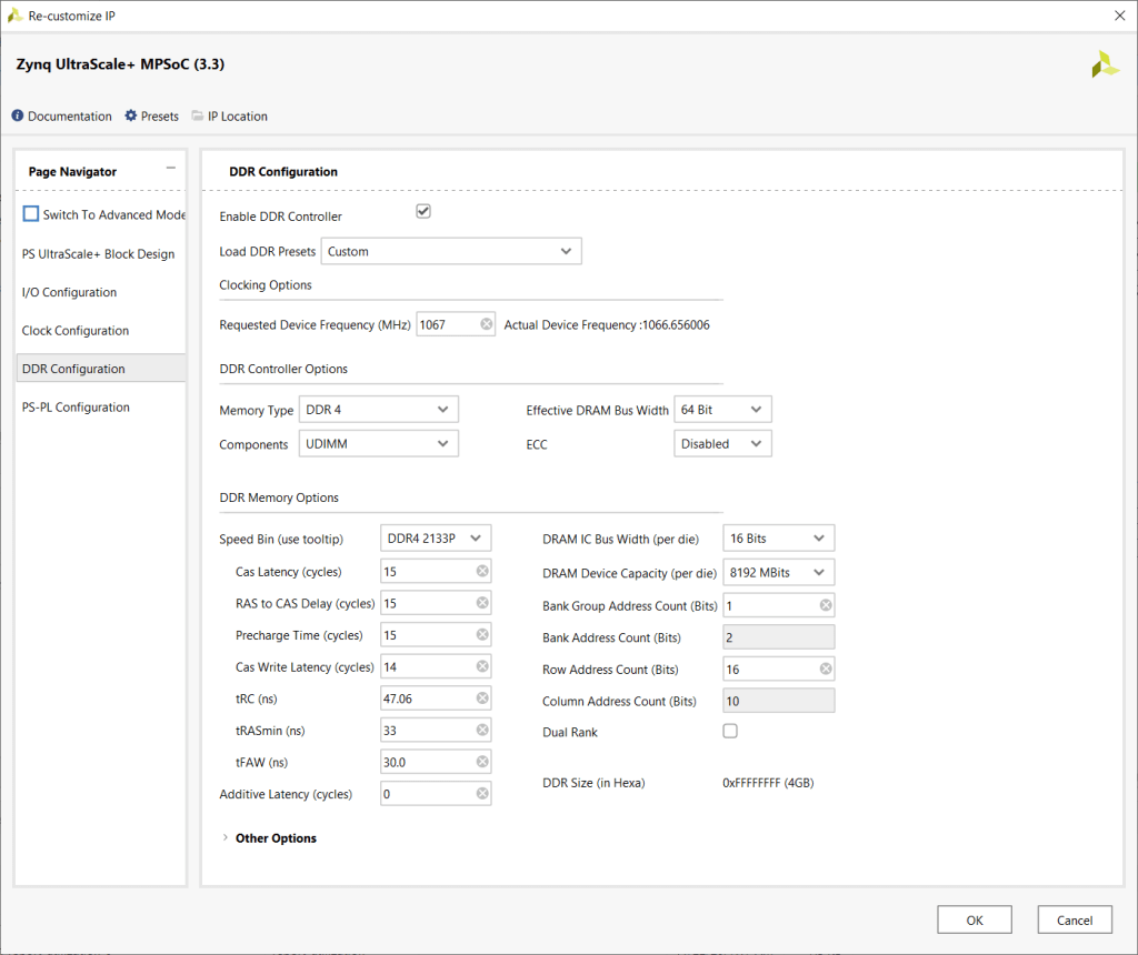
Fig 5: DDR Settings in Zynq UltraScale+ MPSoc IP
- The PL to PS interrupt is set to be level-sensitive by default, and the PS latches the interrupt signal. This interrupt signal from the PL needs to be held high for at least four (4) clock cycles of the GIC (Generic Interrupt Controller).
- Xilinx AR# 50572 was useful in implementing the interrupt handler in the APU.
References
- ZCU106 Evaluation Board – Xilinx User Guide – UG1244 (v1.4)
- Zynq UltraScale+ Device – Xilinx Technical Reference Manual – UG1085 (v1.9)
- Zynq UltraScale+ MPSoC Software Developer Guide – UG1137 (v10.0)
- Zynq UltraScale+ MPSoC: Embedded Design Tutorial – UG1209 (v2019.1)
- Xilinx ZCU106 Software Install and Board Setup – XTP4976
- PmodGYRO Reference Manual – Digilent
- Digikey I2C Master (VHDL) – eewiki Logic – by Scott Larson
- STMicroelectronics AN3393 Application note – L3G4200D: three axis digital output gyroscope
- STMicroelectronics L3G4200D: MEMS motion sensor datasheet
- STMicroelectronics TA0343: Technical Article
- Xilinx AR#71961 – Xilinx Answer Record regarding PS DDR4 memory settings
- Xilinx AR50572 – Xilinx Answer Record – Pl_timer_intr_test.c
- Xilinx Xcell Journal – How to use interrupts on the Zynq SoC by Adam P. Taylor
